Previously Published July 2009
Many anticipate that the next upturn in the semiconductor industry is around the corner. But when? And how? At some level we understand that each successive cycle entails new approaches and methods, winners and losers.
Winners develop new technologies during the slump and use them to get ahead (i.e., of competitors) in the next wave. The downturn presents a fresh opportunity to reflect on trends in the industry and perhaps perceive shifts in direction.
THE CHALLENGES AHEAD
Let’s take a moment to peer a bit into the future and outline a few challenges it presents for microconnection technologies. In tuning our antennae to detect new currents in the ether, we sense the beginnings of a possible wave of change in manufacturing protocols.
It appears here and there as full automation so complete and well-integrated that processes seem to run themselves. That is to say, the factory can run with the lights turned out and without direct human intervention.
LIGHTS-OUT IS NOT NEW
The concept of lights-out manufacturing is not new, but its time may have come. If so, what does it mean to us in the contactor, socket and probe industry?
Lights-out automation would have a significant impact on semiconductor electronics. It transcends differential labor rates and breaks the race to lower labor cost venues. Manufacturing can be done anywhere: close to development to accelerate learning; close to the market for fast response; or in IP friendly environments.
More importantly, it frees-up resources to focus on rapid learning. A steep learning curve is particularly important in semiconductor electronics, where a competitor who falls a few percentage points behind the curve may be out of manufacturing in a short period of time.
A LESSON FROM INTEL
Take a lesson from Intel, a perennial manufacturing powerhouse that has increasingly moved toward lights-out automation in semiconductor production.
This approach allows people to concentrate on improving the tools and processes instead of moving WIP around the wafer fab1. Tools and equipment are standardized to allow reuse and rapid reconfiguration.
The automation and standardization, coupled with Intel’s copy-exactly strategy, preserves and accelerates learning. In essence, manufacturing is a learning machine that can be used as a formidable competitive weapon.

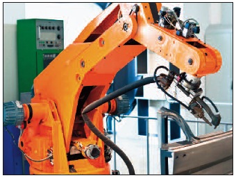
The simplest implementation of lights-out manufacturing is the replacement of a human arm with a robotic arm.
Lights-out manufacturing has been attempted before with limited results. Mea culpa, I spent the late 1980s at the IBM Manufacturing Research Center, dedicated to accelerating IBM’s learning curve. Lights-out manufacturing, as it was understood at the time, largely involved mechanization of manufacturing processes.
In a sense, the simplest implementation involves replacement of a human arm with a robotic arm. Research centers at that time explored advances in robotics and automation. The outcome of all these efforts was often inflexible mechanization rather than intelligent manufacturing.
EARLY ATTEMPTS FIZZLED
Early attempts at lights-out automation fizzled because people in manufacturing tend to perform more than mindless mechanical movements. People in manufacturing are involved in a complex set of interactions involving observation, problem solving, judgment, rapid reconfiguration, and learning.
Without people on the factory floor, who will detect and eliminate snags and problems in manufacturing? Who will see that something “doesn’t look right”? That a misaligned loader is causing jams in product flow? Or that a dirty socket is causing retest?
To reap the benefits of lights-out manufacturing, the semiconductor industry needs more than mechanization. A standardized means of transport is central to automation,
As reviewed in a recent MicroConnections article, 2 Test-in-Tray can do for the backend what the single wafer FOUP did for the wafer fab. Beyond transport, standards for interfaces to equipment, such as the test cell, are needed.
Processes, measurements and tests must be extremely reliable, requiring virtually no maintenance. Everyone in the industry is impacted, including semiconductor manufacturers, fabless IC companies, MEMS suppliers and OEMs.
So, what does this have to do with connectors, sockets, and probes? Plenty! The semiconductor backend is a major market for micro-connectors of all kinds. The requirements are as demanding as the margins are attractive. Clearly, a paradigm shift toward lights-out automation in this sector is important to us.
MEETING THE CHALLENGE
To meet the challenge, significant innovations are needed to overcome impediments to maintenance- free automation.

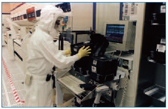
Intel is the leader in standardized processing in the semiconductor industry (Intel photo)
For example, sockets and wafer probes are notoriously temperamental, requiring attention, alignment and cleaning. Retest of poorly contacted parts makes a mess of product flow.
Fixturing is expensive and often incompatible across handlers and testers. Burn-in sockets and ovens are not easily compatible with full automation.
Connectors and sockets are often custom designs that are expensive, long-lead items. These challenges are an opportunity for the test, socket and connector industry to provide enabling solutions toward burn-in and test environment that lends itself to lights-out automation.
STANDARDIZED TRANSPORT PROTOCOL NEEDED
A standardized transport protocol is essential for full automation of backend burn-in and test. A tray format for burn-in and test of arrays of devices allows automated transport throughout the processes including probe, burn-in, test, trim, reflow, mark, sort and tape.
With standard interfaces, the tools and equipment can be rapidly adapted and reconfigured. Fixtures and change-over times are minimized. Process flow of bar coded trays can be handled automatically with minimal intervention.
Obviously, socket or probe downtime is a real impediment to full lights-out automation. Low or zero maintenance sockets, fixtures, and contactors are required. Self-cleaning and self-aligning contactors would ease the problem of eliminating manual intervention for maintenance.
Continuing increases in ball/pad density place further demands for reliable operation on contactor technologies of the future.
LOOKING TO THE FUTURE
Looking to the future, flip-chip-, wafer-level packaging and stacked chips will place additional demands on contactor technology capable of supporting the higher contact density and automatic handling.
Improvements in technology for contactors, sockets, handlers and probes are needed to enable full automation of semiconductor backend production.
Some level of cooperation and agreements on standards and protocols in necessary. The technical community has seen the need and is beginning to respond. SEMI has organized CAST aimed at standards and improvements in the wafer test cell.
MicroConnections has initiated a Test-in-Tray User Group to explore standards and protocols in burn-in and test. More coordinated activity in this area is vital to our industry
REFERENCES
1Excerpted from a VLSI Research interview with Tom Franz, July 25, 2007. 2T. Di Stefano in MicroConnections, Vol. 2, Nr. 4.


